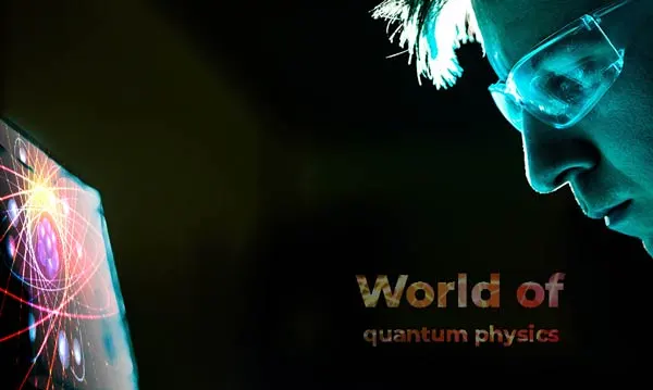
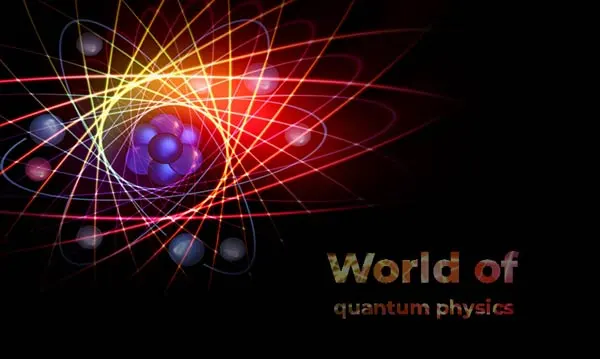
What is photonics? – Polish contribution to the universe of photonics
Photonics is the electronics of the 21st century. Is it really true? What is the Polish contribution to the world of photonics?
Photonics is a very extensive field of science, which includes development of image acquisition and processing techniques, construction of measuring devices using electromagnetic radiation and development of image processing techniques. If you are interested in the subject of photonics – Let’s begin!
In this article you will learn:
- What is photonics? Definition and principles of photonics
- Application of photonics
- Polish photonics engineer – huge potential and development prospects for the science of photonics
- Polish contribution to the development of the science of photonics
- What to do after photonics graduation? Who is a photonics engineer?
- The best academic centers in Poland where you can study photonics
- Photonics in Poland – where are we?
- Photonic research in Poland
- Integrated photonic systems – what are they?
- What is optoelectronics and where is it used?
- Progress in optoelectronics
- The best job offers only in optoelectronics
What is photonics? Definition and principles of photonics
What is photonics? By definition, it is a different kind of physics that deals with light with light waves. It is a science that deals with the generation, detection and manipulation of electromagnetic waves with wavelengths in the range visible to human light and beyond. Photonics is an interdisciplinary field of science that combines the achievements of optics, electronics and computer science. It is in some sense the evolution of electronics using photons instead of electrons. It deals with everything that is related to photons and light manipulation.
Definition of photonics
Photonics investigates various aspects related to the light wave, such as its properties, interaction with materials, optical phenomena and how these phenomena can be used to create advanced technologies.
Photonics has great potential for the development of modern technologies and is used in many areas of life, such as industry, medicine, telecommunications and science.
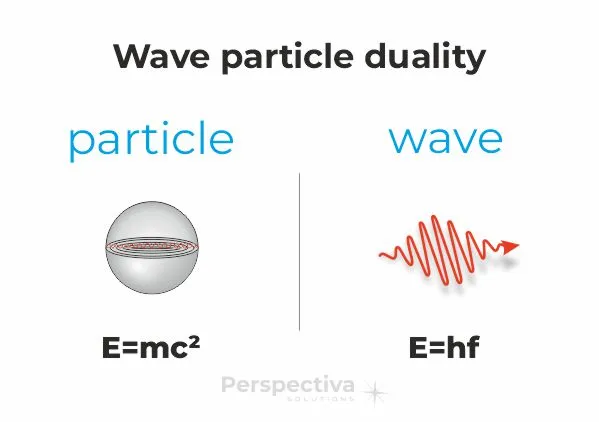
Principles of photonics - particle-wave duality
Principles of photonics in several words
Light has a dual nature also known as wave-particle duality. What does it mean? Light has the nature of both a continuous electromagnetic wave and a particle (photon). The type of acting nature of the light depends on the type of interaction observed. For example, light that is refracted through a lens or diffracted at the edge of a hole exhibits a wave nature. The light produced or absorbed by semiconductor devices such as a laser diode exhibits the particle nature of light.
Application of photonics
What does photonics do? - the field of photonics
- Laser technologies
- Optical fibers and waveguides
- Optical detectors, photovoltaic systems, cameras
- Quantum computers
- Optics
- Opto-mechanics
- Lighting systems
- Microscopy
- Displays (eg: OLED, QLED)
- Light sources (e.g. LED)
- Spectroscopy and spectrometry
List of photonics applications in industries:
- IT and telecommunications – photonic silicon is used not only in telecommunications networks, but also in optical computers and infrared systems or cameras, and photonic integrated circuits used in telecommunications networks and quantum computers
- Industry – laser cutting, drilling or engraving with much greater precision and accuracy
- Medicine – diagnostics, therapy, imaging of changes taking place in the human body
- Photovoltaic industry – more efficient solar cells
- Automotive and robotics – photonic chips for the automotive industry
- Agriculture and forestry – photonic techniques used e.g. for observing and recognizing the condition of plants and animals
- Cosmetology – photonic laser – an innovative device designed to strengthen and speed up the time of hair care treatments
Photonics is also used in aviation and defense, construction and the mining industry.
Polish photonics engineer – huge potential and development prospects for the science of photonics
Photonics is becoming a key technology for acquiring, processing and transmitting information. Interestingly, today its application is very wide, and it has a chance to become a development lever for many other industrial sectors. This is a field with great potential and a prospect for the development of science. Photonics has been successfully used in information technology and telecommunications. In industry, for example, laser cutting, drilling or engraving is done with much greater accuracy and precision. In turn, in medicine, resonance imaging, tomography or other tests that allow for less invasive access to the human body are the effects of rapid technological progress. Modern surgical tools such as fiber optic probes are a great opportunity for a breakthrough in the fight against cancer.
What’s more? Photonics is also photovoltaic technology, i.e. more efficient solar cells that allow you to reduce energy consumption. It is a field that also opens up great development opportunities for other industries such as: aviation, defense, robotics, automotive, construction, mining, space and modern agriculture, forestry and cosmetology.
Polish contribution to the development of the science of photonics
The first fiber telecom line in Poland was built in Lublin. The research team of the Optical Fiber Technology Laboratory of the Maria Curie-Skłodowska University is considered to be the creators of Polish optical fiber photonics. It was here, in 1979, that the first fiber-optic telecommunications line in Poland was built. The big success of Lublin scientists initiated the extremely rapid development of fiber optic technology throughout Poland. Today, many research institutions, both in Poland and abroad, use their experience. Several companies in the field of photonics are thriving in Lublin. One of them is SDS Optic. Their products are fiber optic sensors for diagnostics of breast cancer.
The foundations for the construction of the laser were laid by Albert Einstein, who formulated the theory of stimulated emission of radiation. This phenomenon was first observed in microwave domain, which became an inspiration to build a laser. The LASER acronym itself comes from the English: Light Amplification through Stimulated Emission of Radiation. It is generally acknowledged that the first laser was constructed by Theodore Maiman of the Hughes Research Laboratory in California, and his invention worked for the first time on May 16, 1960, it was a laser built using ruby crystal. The first Polish laser was put into operation on August 20, 1963 at the Military University of Technology (WAT), at the Faculty of Electroradiotechnics, at the Department of Fundamentals of Radiotechnology headed by Maj. Zbigniew Puzewicz, PhD.
Laser microfusion
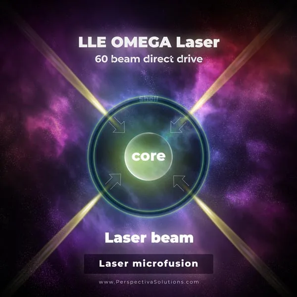
Another interesting figure worth knowing about is General Sylwester Kaliski. Professor of exact sciences and the commandant-rector of the Military University of Technology, who in the mid-twentieth century worked on the phenomenon of laser microfusion. Microfusion technology is a very promising source of clean thermal and electrical energy, although today it is more likely to build a new type of power plant based on fusion carried out in an external magnetic field in devices called tokamaks.
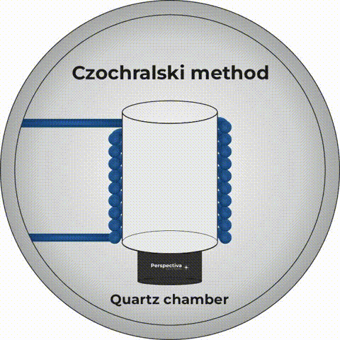
The Czochralski method allows for extraction of crystals
The Pole who probably had the greatest influence on photonics in the world is prof. Jan Czochralski. This specialist in materials science and chemistry, born on October 23, 1885 in Kcynia, developed a method of growing crystals. To this day, it is commonly called by his name. The Czochralski method allows for extraction (as the crystal production process is called) of crystals used in both electronics and photonics. To this day, all processors and active media, i.e. “hearts”, of the so-called solid-state lasers are produced using this method.What to do after photonics graduation? Who is a photonics engineer?
As mentioned above, photonics is the science dealing with light. Some of the goals that specialists in this industry often set themselves are the development of innovative products for medicine, telecommunications, IT, production and construction. Photonics engineers are responsible for significant scientific discoveries, from light that can cut plastic to ultra-precise lasers used in delicate eye surgeries
A photonics engineer is someone who creates and improves systems and products that use photonics – lasers, optics, fiber optics and imaging systems. They check performance by testing whether the system is working properly. They also shape modern technology by developing experimental products that will eventually be perfected for everyday use, including e.g. solar cells or solutions for manufacturing electronics. However, that’s not all! Photonics engineers also create prototypes to determine whether their ideas are plausible.
- Working in the manufacturing industry, they create easier and time saving ways to produce products or systems for assessing their quality, g. vision systems, often using artificial intelligence. They can also design optical materials to make the factory more energy efficient.
- In a company that produces electronics, photonics engineers determine, for example, the energy efficiency of television sets or the quality of emitter matrices by testing crystals.
- In the military, lasers are used for navigation, providing range information for weapons and missile targets, to shoot down drones, and to study hazardous substances.
- In medicine, lasers are used in many diagnostic and therapeutic procedures, as well as for performing delicate operations on the eye or other parts of the body. For example, femtosecond lasers are used to incise the cornea in cataract surgery.
Important! A lot of time is spent researching new solutions in this fast-developing field. Photonics engineers need to stay up to date with the discoveries and research of other engineers, which is why they often participate in conferences with specialists from other sectors to share knowledge and learn about changes taking place in the world of photonics.
There are two career paths open to graduates of photonics. They can work in the commercial sector in technology companies. Or they can continue the path of scientific work, both in domestic and foreign research centers. Working time in Poland is a typical 40-hour working week, although overtime is sometimes necessary to meet research project deadlines. It also happens that in the case of carrying out work in research institutions with the use of complex and sparse infrastructure, it is necessary to carry out the experiment in a limited time window. It takes commitment and sometimes dedication. Traveling abroad is also often a must, as the work is often carried out by international teams. The language of photonics engineers is most often English. Photonics is a typical field of the so-called deep or advanced technologies (deep-tech). Therefore, many engineers decide to continue their education at doctoral (PhD) studies.
The best academic centers in Poland where you can study photonics
- Warsaw University of Technology, Faculty of Physics
- Military University of Technology, Institute of Optoelectronics
- Wrocław University of Technology, Faculty of Electronics, Photonics and Microsystems
- Nicolaus Copernicus University in Toruń, Faculty of Physics
- University of Maria Curie Skłodowska University in Lublin – especially in the field of fiber optics technologies
Depending on the selected academic center, photonics classes are grouped into six thematic blocks: physical, mathematical and IT, technical, major and other.
Photonics in Poland - where are we?
The implementation of the goal, which is the development of optical fiber technology and photonics in Poland, has become the basis for the creation of the Photonics and Fiber Optic Cluster – Polish Center for Photonics and Fiber Optic and Poland’s achievement of a competitive advantage in the field of modern technologies of the future. Analyzes were carried out on the markets with respect to the direction of development of the aviation industry, modern management methods, and the growing demand for organic technologies, including fiber optics, was indicated.
The demand for software enabling the design of optical and optomechanical elements, systems and devices is huge in Poland. What’s more? The interest in this type of software in our part of Europe is growing at a very fast pace. This, in turn, translates into a rapidly growing number of orders, clearly indicating the growing demand in this area.
According to market research conducted indirectly on the basis of the analysis of reports and directly during conversations with entrepreneurs and on the basis of popular science articles and media reports, they indicate that a very important need is to provide services in the field of technology transfer and research in the field of photonics, from research units to industry. They also include the development of research procedures, the implementation of new solutions as well as the adaptation of application research to the growing demand for photonic technologies.
Every year, there are more and more companies in our country that use the potential of technology in this area. Various types of observation devices, reconnaissance and targeting systems have an impact on the growing position in the defense industry. However, the use of optoelectronic devices outside the military is also growing. For example, a renaissance of civilian optoelectronic devices can be observed in devices such as smartphones. In addition, photonics is increasingly used in communication systems and in materials manufacturing and processing systems.
However, despite good development prospects, there are still many barriers in Poland related to the implementation of modern solutions. There are no large Polish companies that would stimulate the development of modern technology in the country. There is also a shortage of mid-level system integrators and manufacturers of highly integrated optoelectronics, e.g. integrated optoelectronic circuits, which may be the basis of future optoelectronic devices.
Photonic research in Poland
Although research on such devices is being conducted in the country, there is still a lack of scientific and industrial centers that would be able to use the results of research and the effects of Polish medium-sized producers. In order to respond to this need, initiatives have been taken in recent years to build several new research and development centers focused on cooperation with industry. These are:
- CEZAMAT – Center for Advanced Materials of the Warsaw University of Technology CEZAMAT is a center with a unique base of cleanroom laboratories focused on the development of new materials for photonics and electronics. It also has the necessary office facilities and excellent administrative support.
- ENSEMBLE3 – Center of Excellence ENSEMBLE3 is a center established as a joint initiative of the University of Warsaw and ITME (Institute of Electronic Materials Technology). Our CEO, Krzysztof Jakubczak , participated in the development of the strategy for the creation of this center.
- CENTERA – Center for Terahertz Research and Applications This is a center that focuses on technologies working in the terahertz range.
Associations supporting entrepreneurs and institutions are also very important in the photonic ecosystem. The most important ones include PPTF – Polish Technological Platform of Photonics and the National Laboratory of Photonics and Quantum Technologies NLPQT.
Integrated photonic systems – what are they?
Integrated photonic circuits are nothing more than a direct equivalent of electronic integrated circuits that we have known for many years. The key difference at the conceptual level is the fact that in integrated electronics the carrier of information and energy is an electron. In photonics, it is a photon – a particle representing a quantum (portion) of energy of light.
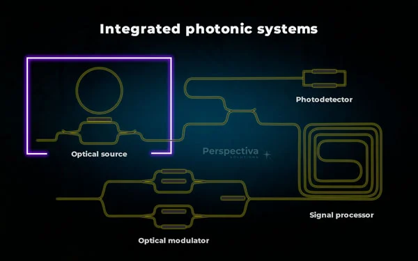
The integrated optical system can be used in many different applications, which increases its availability, reduces costs and minimizes the time spent on research and development. Using the same chip, you can perform mathematical operations, implement artificial intelligence and machine processing systems, sensor networks on a chip, imaging systems and manipulate the quantum states of light.
However, it is worth noting the differences between electronic and photonics integrated circuits:
- Speed of action Photonic systems work much faster, which creates hope for much greater computing power of the future quantum computers.
- Energy saving Photonic systems have the potential to consume much less energy
- Security In principle, it is impossible to “eavesdrop” on photonic systems as is routinely done in electronic systems. A potential intruder is detected immediately. What’s more, in the case of, for example, an attempt to intercept information in a fiber-optic network, it is also immediately known where an attempt was physically made to break into the network.
Integrated quantum photonics uses classical integrated organic, inorganic technologies and devices for quantum applications. However, integration at the chip level is crucial to scale up and translate demonstration prototypes from labs to real-world technologies. Efforts in the field of integrated quantum photonics are large-scale and involve the development of quantum circuits that can be integrated monolithically, hybridly or heterogeneously.
According to the researchers, there is an urgent need for major investments to be able to train the next generation of engineers in this sector. There is a growing demand for scientists and engineers with extensive knowledge, both in the field of quantum mechanics and technological applications. Investment in the education of the next generation will certainly contribute to pushing the boundaries of science and technology.
What is optoelectronics and where is it used?
Optoelectronics deals with the engineering of systems and devices that emit, model, and transmit or detect light including electronics that works together. In addition, he also deals with the construction and application of all kinds of devices and apparatuses for the emission and detection of light. It is a field of technology that uses the properties of light to process information. Thanks to optoelectronics, it is possible to obtain, collect, transmit, process and present information using various elements such as photoelectric detectors, laser CD factors, Irda infrared ports, LCD displays or plasma displays. In other words: optoelectronics is a combination of optics and electronics.
Various optoelectronics can be distinguished, such as:
- fiber optic,
- imaging ,
- photovoltaic,
- IT,
- laser optoelectronics.
It has a number of different applications in many fields such as chemistry, physics or electronics. Optoelectronics is used in fiber optic telecommunications as well as in automation and robotics. Thanks to it, it is possible to create computer networks resistant to interference. It also allows you to store data on CDs or DVDs. It is also successfully used in photovoltaics, which deals with the processing of sunlight into electricity.
Progress in optoelectronics
Optoelectronics is one of the key areas supporting the development of the Polish economy and defense. It plays a key role in supplying important elements of the country’s defense system and equipping the Polish army. The leader of innovation in the Polish optoelectronic industry is the Warsaw-based PCO SA, which has been specializing in the production of products belonging to the individual soldier’s equipment and combat vehicles using optoelectronic sensors for over 45 years. The previously unavailable MT-1 thermal imaging monocular was also developed there. The combination of experience and competence of specialists has resulted in the creation of a device unprecedented not only on the Polish market, but also on the world market. From the perspective of many years, it can be seen that the developed, modern optoelectronic technologies are innovative ideas that meet the expectations of equipment users and the industry.
The best job offers only in optoelectronics
Industries where graduates of optoelectronics can count on employment:
- Enterprises and research units that carry out projects related to the design, construction and use of elements of satellite devices or lasers
- Research and development institutes
- Public and private universities educating specialists in the field of space and satellite technologies
- Institutions of the Ministry of National Defense
- Health care units in the field of operation and maintenance of laser medical devices
- Companies using advanced technical means of transport
- Companies dealing with the storage and liquidation of hazardous substances
- And territorial defense units in the field of service and maintenance of security systems
Are you interested in the topic of photonics? Also check out our contract electronics manufacturing services!
Suggested articles related to the topic of photonics:
Popular articles on our blog:


Comments (8)
Comments are closed.
Mike RICHARDSON
11 January 2023Perspectiva Solutions awesome work you did and it’s just a reminder that any quick look into Polish technical capability must include Łukasiewicz. it’s really important that if you’re mentioning Polish Photonics to include Łukasiewicz – Institute of Microelectronics and Photonics.
#lasers #photonics #semiconductors #defenseindustry #quantumtechnology
Kamil Pierściński
11 January 2023Tkanks Mike! Much appreciated 🙂
Mike RICHARDSON
11 January 2023Kamil Pierściński when we show the video about what you doing with photonic integrated circuits world-leading research, will be exciting
Łukasiewicz - Institute of Microelectronics and Photonics
11 January 2023Thank you Mike for mentioning us 🙂 Since we’ve been mentioned here – we’re taking this opportunity to add something to the text above – it was in our Institute, exactly in 2009, that the first quantum cascade laser ( hasztag #QCL ) in Poland emitting radiation with a wavelength of 9.4um and the first measurement laboratory in Poland were created, allowing for comprehensive testing of devices emitting in the infrared range. QCLs are key photonics devices, especially IR photonics.
Łukasiewicz – Institute of Microelectronics and Photonics. – Scientific research and developmental work | micro-, nano- and optoelectronics, nanophotonics, microwave electronics
admin
11 January 2023Thank you Łukasiewicz – Institute of Microelectronics and Photonics for your contribution. Spectacular achievement. Congratulations! Good to know and good luck in the commercialization of your lasers.
admin
11 January 2023Thank you for your comment. Indeed, there’s a lot more of the contributors. And the longer we think the more of them we’d like to add 🙂
Here, we just wanted to create a quick-look publication to show that the sector is important for Polish science and economy. The fact is there’s a lot more of the important scientists and companies to recognize. Due to the specificity of the publication we decided only to “give the flavor”. We do hope though that one day more extensive market report on “Polish photonics” could be created.
rafalczura
17 January 2023It’s exciting to hear that Poland is making contributions to the universe of photonics. The country has a long-standing tradition of excellence in science and technology, and its researchers and engineers have been actively involved in advancing the field of photonics. With its rich history in optics and photonics research, Poland has been making valuable contributions to areas such as telecommunication, optoelectronics, biophotonics, and quantum optics.
I look forward to seeing further advancements and breakthroughs from Poland and other countries in the field of photonics, as it continues to play a crucial role in shaping the future of science, technology, and our modern society.
EcoRT_90
12 August 2023Wow, I’m impressed with this article! I always thought that photonics is such an abstract field, and here I find out that it is photonics that is responsible for our light in telecommunications networks. It’s interesting that Poland has a word to say here. It seems that this is not only a dry theory, but also a lot of practice – applications in medicine or industry. Perhaps the most fascinating thing is that these innovations in photonics may revolutionize many fields in the future. I keep my fingers crossed that Polish scientists will continue to give great results!